
 |
 |
 |
 |
 |
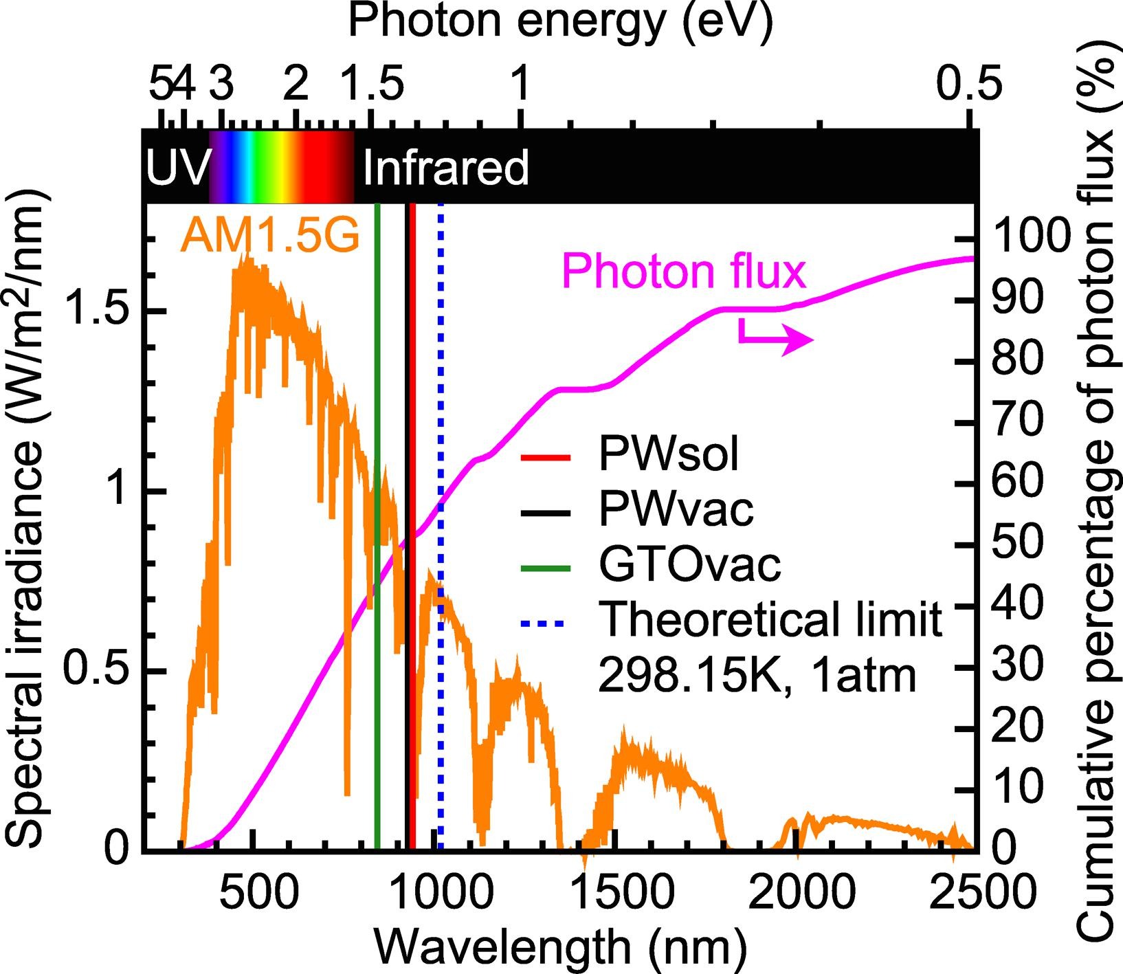 |
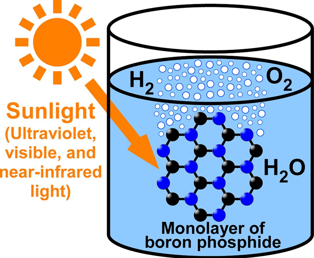
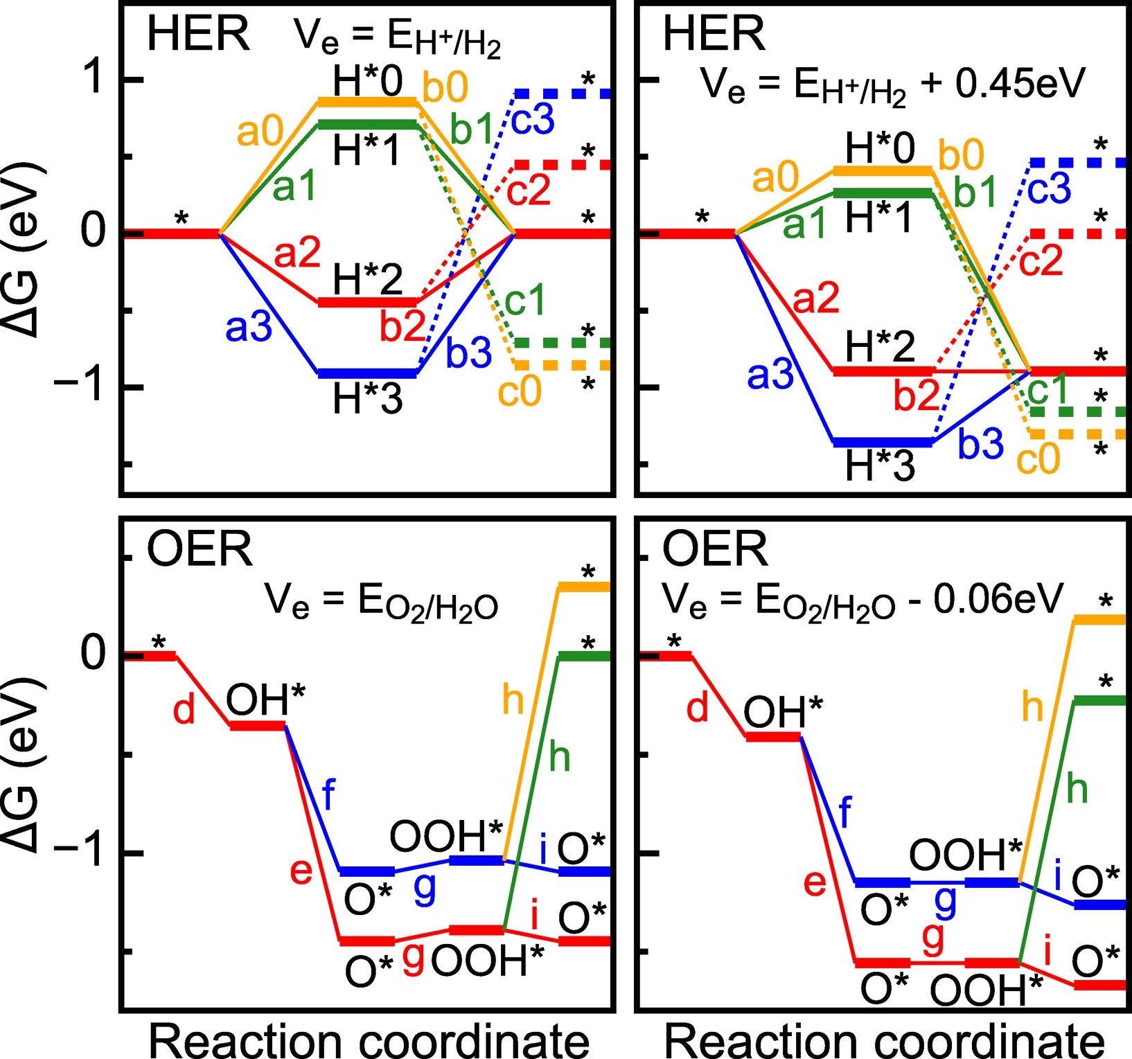
Abstract: Recently, hydrogen generation by water-splitting photocatalysts is attracting attention as a sustainable and clean energy resource. Photocatalytic hydrogen-generation systems are much simpler, cheaper, and easier to scale up than the coupled systems of electrolysis and solar cells, wind-power generation, etc. However, photocatalytic hydrogen generation is currently inefficient. This paper proposes the monolayer of boron phosphide as a stable highly-efficient water-splitting photocatalyst by high-precision density-functional theory calculations using a HSE06 functional with a solvent effect. The monolayer of boron phosphide has a direct allowed energy gap of about 1.4 eV, and functions as a one-step excitation photocatalyst. It absorbs sunlight with wavelengths below about 890 nm (ultraviolet, visible, and near-infrared light) and produces both hydrogen gas and oxygen gas from water at a suitable pH condition. By calculating the overpotentials of hydrogen and oxygen evolution reactions, its photocatalytic effectiveness was confirmed. The monolayers of boron phosphide will realize green hydrogen revolution. © 2022 Tatsuo Suzuki
Abstract: Group III-V compounds are very important as the materials of semiconductor devices. Stable structures of the monolayers of group III-V binary compounds have been discovered by using first-principles calculations. The primitive unit cell of the discovered structures is a rectangle, which includes four group-III atoms and four group-V atoms. A group-III atom and its three nearest-neighbor group-V atoms are placed on the same plane; however, these connections are not the sp2 hybridization. The bond angles surrounding the group-V atom are less than the bond angle of sp3 hybridization. The discovered structure of GaP is an indirect transition semiconductor, while the discovered structures of GaAs, InP, and InAs are direct transition semiconductors. Therefore, the discovered structures of these compounds have the potential of the materials for semiconductor devices, for example, water splitting photocatalysts. The discovered structures may become the most stable structures of monolayers which consist of other materials. © 2015 AIP Publishing. This article may be downloaded for personal use only. Any other use requires prior permission of the author and AIP Publishing.
Abstract: Graphene nanoribbons (GNRs) are stripes of single layered graphenes with a finite width. The electronic states of GNRs are different by the edge conditions (armchair edges or zigzag edges). The results of tight-binding approximations are that the hydrogen terminated zigzag GNRs are metallic, and the hydrogen terminated armchair GNRs are metallic or semiconducting. But the narrowest hydrogen terminated GNRs are polyacethlenes, that are semiconducting. The reason of this contradiction is that the structures of polyacethlenes are changed by the Peierls transition. Therefore the effects of the Peierls transition of GNRs from polyacetylenes to graphene were examined systematically using density functional theory with structural optimizations. © 2011 American Institude of Physics
Abstract: The mobility of graphene is very high because the quantum Hall effects can be observed even at room temperature. Graphene has the potential of the material for novel devices because of this high mobility. But the energy gap of graphene is zero, so graphene can not be applied to semiconductor devices such as transistors, LEDs, etc. In order to control the energy gaps, we propose atomic monolayers which consist of various materials besides carbon atoms. To examine the energy dispersions of atomic monolayers of various materials, we calculated the electronic states of these atomic monolayers using density functional theory with structural optimizations. The quantum chemical calculation software "Gaussian 03" was used under periodic boundary conditions. The calculation method is LSDA/6-311G(d,p), B3LYP/6-31G(d), or B3LYP/6-311G(d,p). The calculated materials are C (graphene), Si (silicene), Ge, SiC, GeC, GeSi, BN, BP, BAs, AlP, AlAs, GaP, and GaAs. These atomic monolayers can exist in the flat honeycomb shapes. The energy gaps of these atomic monolayers take various values. Ge is a semimetal; AlP, AlAs, GaP, and GaAs are indirect semiconductors; and others are direct semiconductors. We also calculated the change of energy dispersions accompanied by the substitution of the atoms. Our results suggest that the substitution of impurity atoms for monolayer materials can control the energy gaps of the atomic monolayers. We conclude that atomic monolayers of various materials have the potential for novel devices. © 2010 Elsevier B. V.
This paper was first presented at the 14th International Conference on Modulated Semiconductor Structures (MSS14) held in Kobe, Japan, on 23 July 2009.
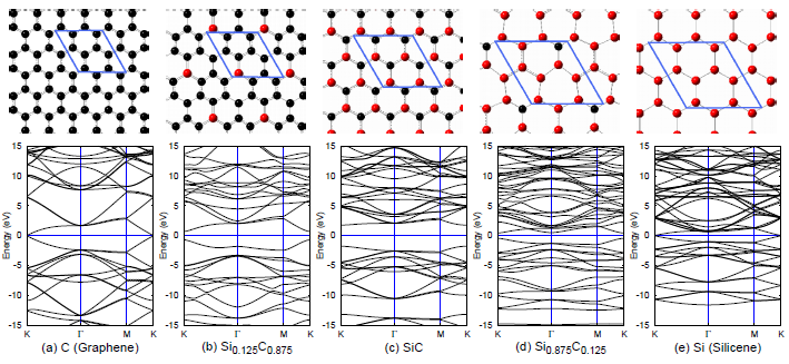 |
| Energy dispersions of atomic monolayers which consist of carbon atoms and silicon atoms. |
Abstract: Hamiltonians that generally describe the effects of strain are proposed. The strain effects can be calculated easily from the unstrained potential using these Hamiltonians. These Hamiltonians are valid when the strain is spatially modulated, and are also valid when the strain exists in a magnetic field. These Hamiltonians can also be used in the improved effective mass approximation. © 2001 The American Physical Society
Abstract: Results of detailed self-consistent calculations for edge states are reported on the energy level structure of wide quantum wires formed by a split gate at GaAs/AlGaAs heterostructures in high magnetic fields at low temperatures. The flattening of the dispersion of edge states (a compressive strip) appears only in very wide wires under limited conditions that the estimated width of the strip is larger than the extent of the edge-state wave function, i.e. the cyclotron radius. © 1998 Elsevier Science B. V.
Abstract: Results of a self-consistent calculations are reported on the energy level structure of quantum wires formed by a split gate at GaAs/AlGaAs heterostructures in high magnetic fields at different temperatures. The electron density associated with partially filled Landau level oscillates spatially to minimize the Coulomb energy and has a characteristic double-step variation near the edge at low temperatures. © 1996 Elsevier Science B. V.
Abstract: Results of a self-consistent calculation are reported on the energy level structure of quantum wires formed by a split gate technique at GaAs/AlGaAs heterostructures in magnetic fields. The confinement potential approaches an abrupt barrier in high magnetic fields even for narrow wires for which it is nearly parabolic in the absence of a field. © 1994 Elsevier Science B. V.
Abstract: A self-consistent calculation is performed for the study of magnetic-field effects on the energy level structure of quantum wires formed by a split gate technique at GaAs/AlGaAs heterostructures. The self-consistent potential and the energy dispersion exhibit a dramatic change when a subband depopulation occures in high magnetic fields. © 1993 The Physical Society of Japan
Abstract: A search has been made for strange matter with a CR-39 track-etch detector with an array of 160 m2, exposed for 8 months at mountain altitude. The non-observation of penetrating tracks places a new stringent upper limit on the flux of strange matter, 2.2×10⁻¹⁴cm-2s-1sr-1 (90% confidence level) in the velocity range β(≡v/c) > 4×10⁻⁵. © 1991 Elsevier Science B. V.
Abstract: A direct search has been made for supermassive relics (heavier than about 1012 GeV/c2) with a 2000-m2 array of CR-39 track-etch detectors deployed underground for 2.1 yr. The nonobservation of penetrating tracks places a new upper limit for the velocity-dependent flux at 3.2×10⁻¹⁶cm-2s-1sr-1, for magnetic monopoles carrying various magnetic charges, for electrically charged relics, and for strange matter. This flux limit corresponds to a limit on the relics abundance of order nx/nγ=10-28 relative to the 3-K photons. © 1991 The American Physical Society